Back to Steve's Home Page
|
THE CALL HOME PROJECT
In 2008, after a winter storm that knocked out the AC power to my area for several days, I decided that I wanted a system that allowed me to use the plain telephone system to interrogate my house from afar using a modem on a laptop. The internet to my home depends on AC power, but very often the plain old phone service remains in service when the AC is lost. I found a single board computer that had both analog and digital I/O, called the Rabbit LP3500, now made by Digi International. The LP3500, with optional prototyping board, seemed just right for my purposes, and I bought one. The prototyping board provides high quality screw terminals for all I/O connections to the LP3500. I will refer to the LP3500 as the "Rabbit" in the following. I also located and purchased a modem card that supported 8-bit (i.e., byte-wide) parallel I/O in a bi-directional data bus.
The Rabbit contains 512KBytes of Flash Memory for its stored program and 512KBytes of SRAM for data. It is programmed in C with the binary downloaded to the Flash Memory so it is a stand-alone computer.
In the Rabbit, the key I/O features for my purposes are 10 bits of digital output (organized as 8+2 with all bits addressable), 16 bits of digital input, 8 analog inputs multiplexed to a 12-bit ADC, and a couple of pulse width modulated output bits. It also has several serial ports that I am not using. Most importantly, 8 of the output bits were open collector (current sinking), which meant that it would be possible to create externally, among other circuits, an 8-bit bi-directional data bus by tying the 8 such output bits to 8 of the input bits; this configuration constitutes a byte-wide bi-directional data bus, a bus compatible with the external modem, and with my future custom peripherals, such as an image sensor.
I possess a Hitachi 100MHz dual trace oscilloscope that I bought some 20 years ago. This is fast enough to follow most logic signals of the 74LS and 74ALS series of integrated logic circuits, my preferred hardware family. The maximum clock speed of the Rabbit, by the way, is about 7MHz, way slower than my external interface circuitry.
I built an interface board for connecting the Rabbit to the modem and to my future peripherals (not determined at the time) in 2008. The next section is a description of this interface, which combined with the Rabbit itself I call the "Rabbit Microcomputer System", or "Rabbit Interface" for short.
So I designed and built the following system:
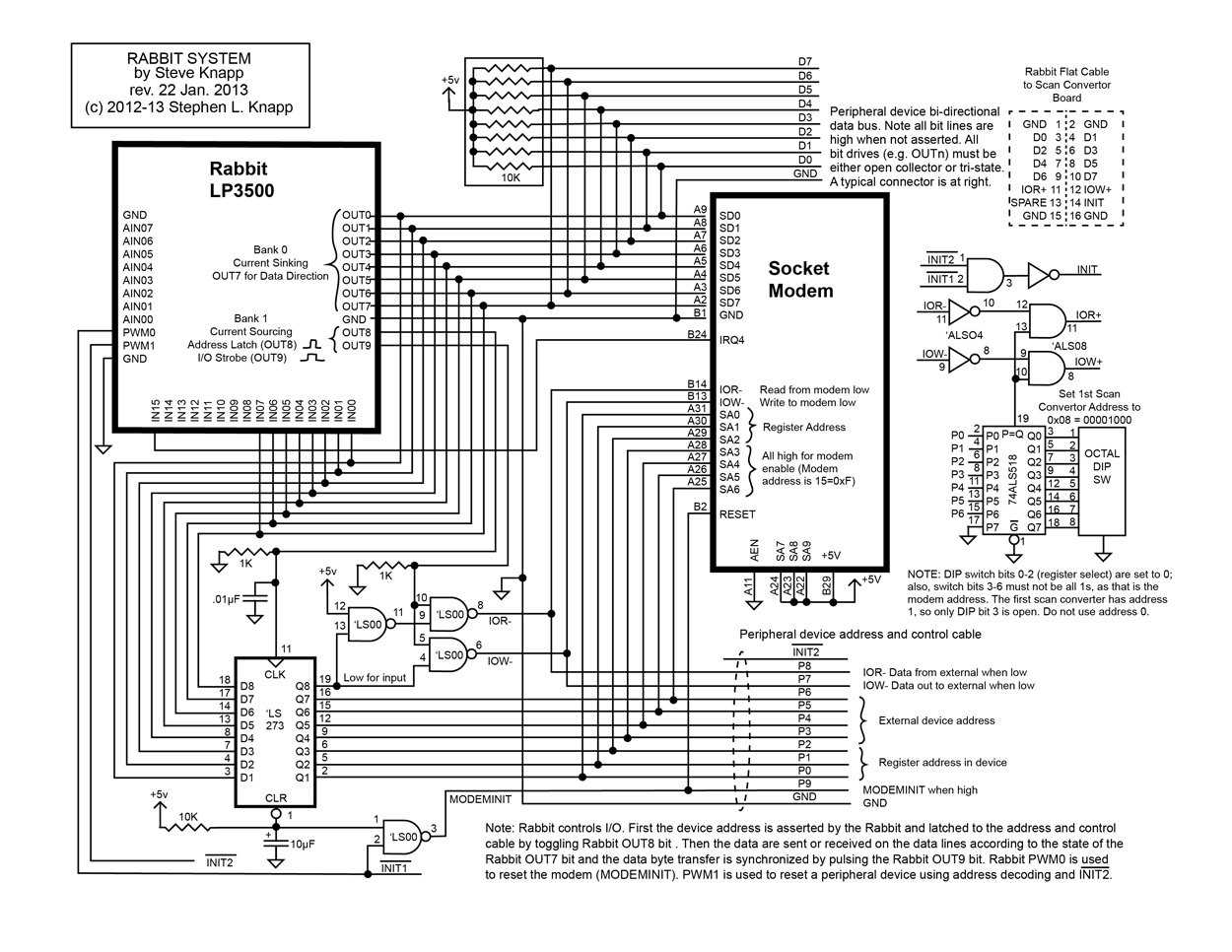
The idea is that the Rabbit LP3500 controls everything (but is itself given commands by telephone via the modem). There had to be an external address bus in addition to the bi-directional data bus because there would probably be one or more peripheral subsystems in addition to the phone modem. To do this using the data bus an byte-wide latch is used to store the address of the external device. One bit of this bus is used to control whether the external device is sending or is receiving the next data byte on the data bus. The two extra output bits, OUT8 and OUT9, are used to control the storage of the peripheral address and the timing of the read or write signals.
Yes, this is pretty damn complicated. . . . And the damn thing did not work. I spent a week with my oscilloscope trying to see what was wrong. Shit, I was baffled. So in early 2009 I dropped the project, and all this work was stuck away out of sight in my spare bedroom lab. Boo Hoo.
But you know something like this doesn't leave the sight of one's brain for long. Every now and then I would look at the schematic diagram (above) and go over the signal timing in my mind. I should be working. . . .So finally this year (2012!) during the summer, I dragged the Rabbit system out of its dungeon and plugged in the Hitachi oscilloscope once again. After tearing my hair for a couple of days, and remembering how it was in the illustrious past at Caltech and other labs, I finally found the problem. A cross-over sliver! Jesus, I should have guessed. It turns out that when a binary command (in the stored program in the LP3500) to change the OUTn bits of the LP3500 is executed, there can be a very brief "spike" on an output bit (remember the slow clock speed of the LP3500), and in my circuit, it was critical on OUT8, which is connected to the clock input to the address latch, a 74LS273 device. The spike was tiny, only about 10 ns and with a peak voltage just at the logic "high" threshold. This "sliver" was just enough to trigger the latch in error. Such a signal is at the very limits of detection on the screen of the 100MHz oscilloscope, particularly because the event is not repetitive. The Hitachi just can't "paint" on the screen phosphor much of this trace; it was visible only in darkness, and I had missed it using a towel during daytime to shield the daylight, which wasn't dark enough. The solution is to add a capacitor to the clock input of the latch, and it is the 0.01μF capacitor in the diagram.
Hooray! It works! So the first thing I did was to add a single semiconductor temperature sensor to one of the analog inputs to the LP3500, so that I can at least get the air temperature at the Rabbit. For controlling the system remotely I add an external USB modem to my MacBook Pro, and I have developed an app using Real Basic that runs on the Mac. Now I can call up the Rabbit from afar. The Rabbit answers the phone, and asks for a password. My Mac app relays this request and when I give the correct password, the Rabbit supplies the temperature. If the password is wrong, the Rabbit hangs up its modem. All of this conversation is handled by the app, which is user-friendly. And the programming of the Rabbit, as a stand-alone, modem-driven data system has been developed and proven. The protocols for operating my complex interface are understood.
Now a single number, the ambient temperature, is easy. What is NOT easy is, say, an image in the house, say of the big central room. And we need something difficult to do. Right, let's go for images. . . .
I started work on the imaging system in September, 2012. In looking at the available sensors and keeping in mind the speed and capability of the Rabbit microprocessor and the modem speeds it seemed logical to separate the project into (a) sensor choice, (b) design and construction of a scan converter (buffer image memory), and (c) building the camera front end, the imager board.
The basic idea of an images sensor is a semiconductor light detector arranged in a two-dimensional array. The sensors in the early cameras at Caltech were built around CCD (Charge Coupled Device) array detectors followed by a separate analog to digital converter (ADC) to produce digital values proportional to the light values in each picture element (pixel) in the array. Thus the output values of the ADC constitute a raw image in digital form. Subsequent computer processing was applied to the raw image data to make a useable image. Technical development since those early days has been stupendous.
At present, very complex camera sensors are available at low cost that not only contain the imaging array but also contain an ADC and a processor integrated into the same large scale integrated circuit chip so as to output formatted image files already processed to correct for many sensor characteristics and inaccuracies; some examples are color correction, black reference, and defect correction. The files are produced by the devices as a high speed stream of data bytes arranged as a raster scan. Most of the easily available devices are made for minature applications, such as mobile phones. The difficulty was finding a device that (1) did not require advanced assembly techniques, for example re-flow soldering, (2) that had a relatively modest image size (like VGA or SXGA), and (3) was stocked by customary distributers (the latter are Digikey.com and Mouser.com).
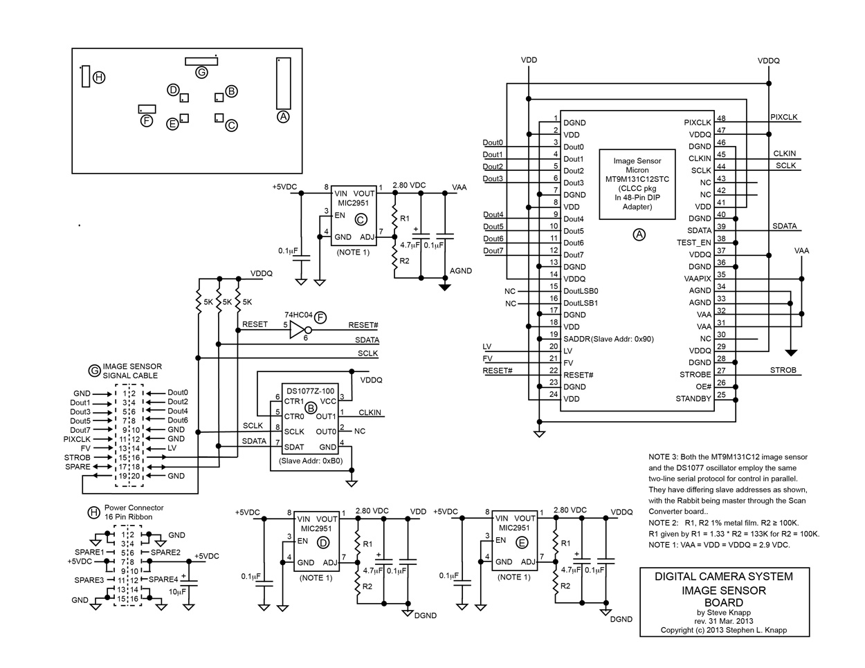
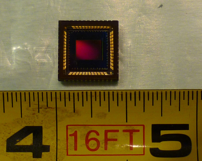 I settled on the Micron© MT9M131C12STC digital image sensor, shown at left. This device provides 1280x1024 images at 15 frames per second using a 54MHz clock. I would favor a device with a smaller image, but this imager can be operated at VGA mode and at other formats. The device is operated using an external clock and the clock can be
slowed both for smaller images and for low ambient light levels. Operated in VGA mode (640x512 px), with color multiplexed to 2 bytes per pixel, a frame (including black border pixels) consists of 673,920 bytes and the maximum frame rate is 30 fps. In its full SVGA mode, the image frame comprises 2,658,432 bytes at a maximum frame rate of 15 fps. The device is very flexible by means of more than 250 addressable registers. For example, the active image area can be set to be any rectangular area within the entire sensor image array, to permit smaller images with adjustable aspect ratios. The maximum data rate of the output byte stream is about 20ns per byte. This high data rate requires a storage buffer, which is called a scan converter. The imager is packaged as a 48-contact CLCC device, which while awkward, is solderable to a suitable adapter or (for the next version) a custom printed circuit board.
I settled on the Micron© MT9M131C12STC digital image sensor, shown at left. This device provides 1280x1024 images at 15 frames per second using a 54MHz clock. I would favor a device with a smaller image, but this imager can be operated at VGA mode and at other formats. The device is operated using an external clock and the clock can be
slowed both for smaller images and for low ambient light levels. Operated in VGA mode (640x512 px), with color multiplexed to 2 bytes per pixel, a frame (including black border pixels) consists of 673,920 bytes and the maximum frame rate is 30 fps. In its full SVGA mode, the image frame comprises 2,658,432 bytes at a maximum frame rate of 15 fps. The device is very flexible by means of more than 250 addressable registers. For example, the active image area can be set to be any rectangular area within the entire sensor image array, to permit smaller images with adjustable aspect ratios. The maximum data rate of the output byte stream is about 20ns per byte. This high data rate requires a storage buffer, which is called a scan converter. The imager is packaged as a 48-contact CLCC device, which while awkward, is solderable to a suitable adapter or (for the next version) a custom printed circuit board.
The scan converter contains a memory into which an image data frame is written on the fly as output in the stream from the image sensor and from which the same image data is read by the Rabbit and sent to the much slower modem for remote transmission. The fast 20ns/byte timing for the memory requires some careful engineering to keep the memory cost reasonable.
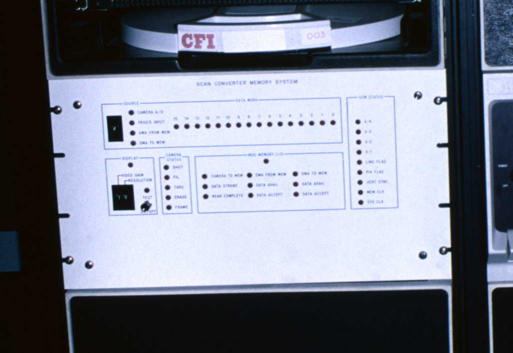
A few of you will know that my first real project as a support technical staff member at Caltech in the mid 1970s was to take over the digital side of the first electronic camera at the Astronomy Department. This was the scan converter for the SIT camera system being developed by Jim Gunn. I had further work with digital camera systems at Caltech through contact with Jim Westphal in Planetary Sciences. Thus I have some background in digital imaging. While the concepts are the same, the advances in integrated circuits, especially in speed and density, have been breathtaking since those early days.
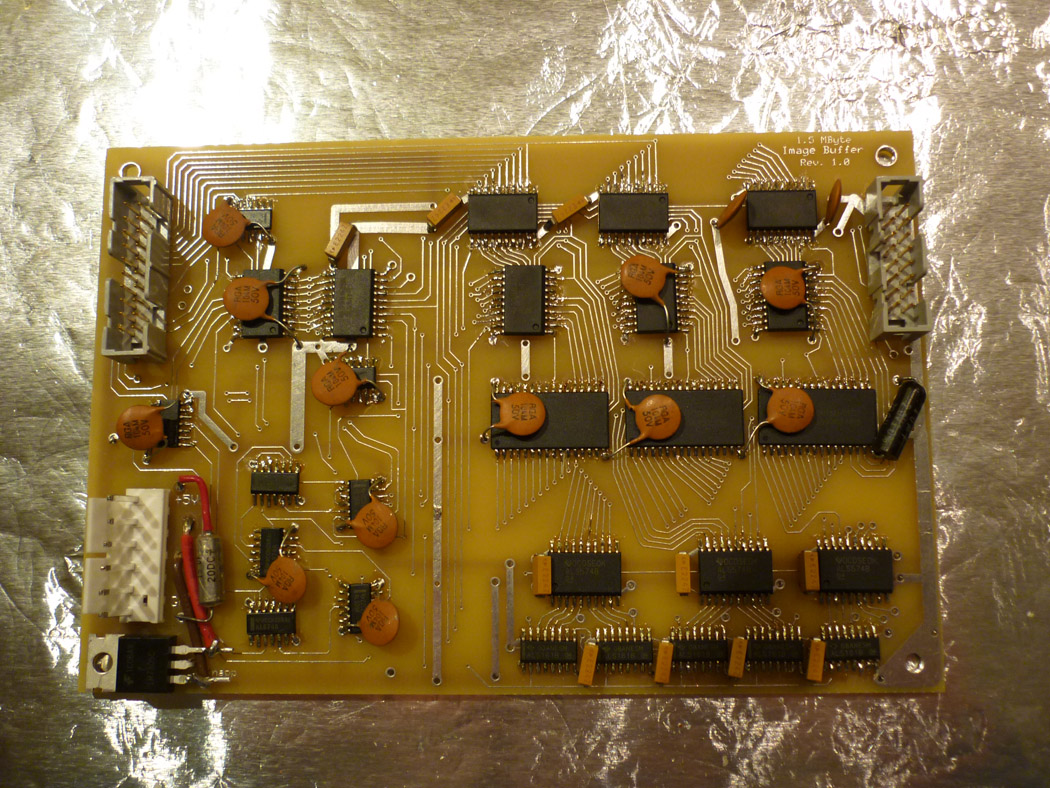
At right is a photo of the digital processing rack for the SIT camera system in 1976 at the 200inch telescope at Palomar Observatory. The scan converter is the white unit on the left part of the rack. It is the scan converter that I put into service. The white chassis is has a standard 19-inch width, which will give an idea of its size. If you click on the image you will get an enlargment of the scan converter. This scan converter had the capacity of a single image of 64 x 512 pixels at 12 bit resolution, for a total memory of 32K x 12 = 393,216 bits. The unit contained 12 PC boards each holding 1024 12-bit pixel values as well as another 10 boards for control and I/O. In comparison, we are now going to describe the modern scan converter. It occupies a single PC board, of similar area of just one in the 1975 unit, and contains all the I/O logic and a memory of 1.5MBytes, that is of 12,582,912 bits, 30 times more. |
 |
The 1.5MByte Scan Converter board.
[Not for the faint of heart.]
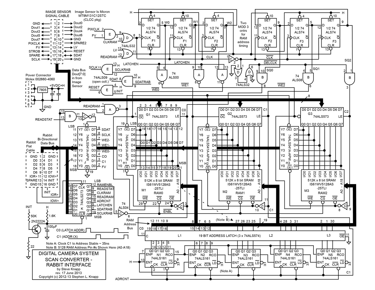
Refer to the following circuit diagram, immediately below. [It may help to open the larger version in a separate window.] Medium and large scale integration over the last three or so decades has made available many integrated circuits (ICs) that serve in data and memory intensive applications such as the scan converter. The memory in the scan converter is made of three identical 0.5MByte ICs. In addition, byte-wide registers and three state I/O stages are common. The memory ICs are found in the lower center of the diagram, with register ICs in support of I/O making three clusters.
Modern IC technology also means that byte-wide, bi-directional data busses are easy, and this structure lends itself to a scan converter with complex buffer memory ICs. A byte-wide bi-directional data bus is like a eight telephone lines that all talk together in either direction and only one party may talk at one time but on all eight lines simultaneously. Sometimes the bus may run in only one direction but has multiple destinations. There are three such busses in our scan converter, and they are shown as heavy wide black lines in the diagram. The upper bus carries the image data from the image sensor (connected externally by cable to the PCB) to registers for sequential writing to the three memory ICs. The middle bus is truly bi-directional as it is the communication path between the PCB and the Rabbit microcomputer. Not only do all data pass on this bus but also all the control signals (mostly from the Rabbit to the scan converter board), and great care is necessary both in the design of the PCB and in the software programming (in the C language) of the Rabbit. Finally the lower bus carries the 19-bit address to the memory ICs during writing or reading operations.
|
The scan converter schematic diagram with corrections found during debugging. Note that because the read and write cycle times of the static ram devices are longer than the fastest pixel readout speed of the imager, it is necessary to divide the entire image frame memory into three devices, accessed sequentially. |
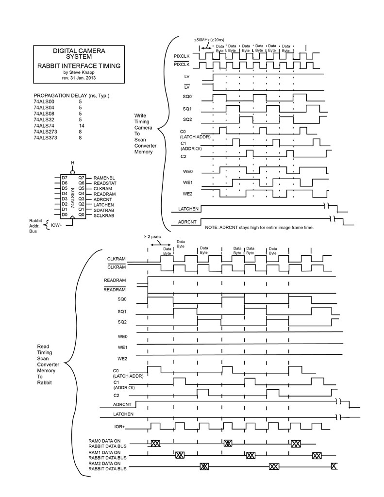 |
Timing diagram of the signals internal to the scan converter on left. The sequential access to the static ram chips uses two separate divide by 3 counters created with the D-type flip flops. |
The timing of the control signals in the scan converter is paramount and critical. Refer to the second diagram, just above, which shows how the reading and writing to the memory ICs and the associated read and write signals interact. As is usual with a scan converter, the reading and writing into and out of the RAM uses sequential, not random, addressing, supplied by a combination of divide-by-three circuits and by a 19-bit counter. There are two ÷3 circuits at the top of the schematic diagram made using D-type flip flops. The 19-bit address counter is at bottom. The board is controlled by the Rabbit by writing to a byte-wide register IC, labelled "K" at lower left. Two signals sent to this register, SCLKRAB and SDATRAB, are relayed by the PCB to the imager board (see below) to control the image sensor. The software in the Rabbit determines whether the Rabbit bus is reading or writing by sending the separate signals IOR+ and IOW+, respectively.
In the past, my digital designs have been constructed using wire wrapping and integrated circuits in sockets in perforated circuit boards. But both the image sensor and the chosen static random access memory (SRAM) ICs only come in tiny surface mount packages. Wire wrapping was ruled out. Surface mount ICs require printed circuit board (PCB) technology. I had done a simple PCB in the late 1970s at Caltech but I had stayed with wire wrapping in the intervening years for professional and for my own projects. So in a sense I was overdue to learn PCB and surface mount technology.
I was happy to discover on the internet that at least one vendor existed that made design and production of a PCB both inexpensive and easy. Expresspcb.com would deliver a very complex 4x6 inch double sided board for under $125, and they supplied free software for laying out the board that was, I found, easy to use and rather elegant. Yet I undertook the PCB knowing full well how ambitious a job it was. Having a printed circuit board, and a crowded, double-sided one at that, as a prototype is pushing the R&D envelope for a home project. In this home at least. Wait, this home is itself also a prototype!
|
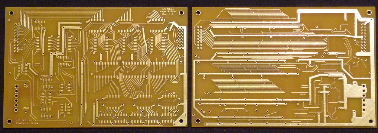
|
The front and back of the bare Scan Converter PC Board. Barely visible in this and later photos are the many "vias" made from plated-through (conducting) holes that connect traces on front and back sides. |
|
|
 |
|
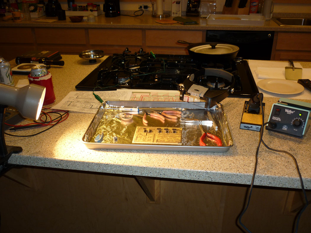
Anti-static soldering station located on the kitchen counter. Note that the baking tray with aluminum foil is grounded (by the wire and clip) as a precaution against static sparks. Difficult to see above the upper right corner of the baking pan is a pair of magnifying goggles, needed for the fine work. |
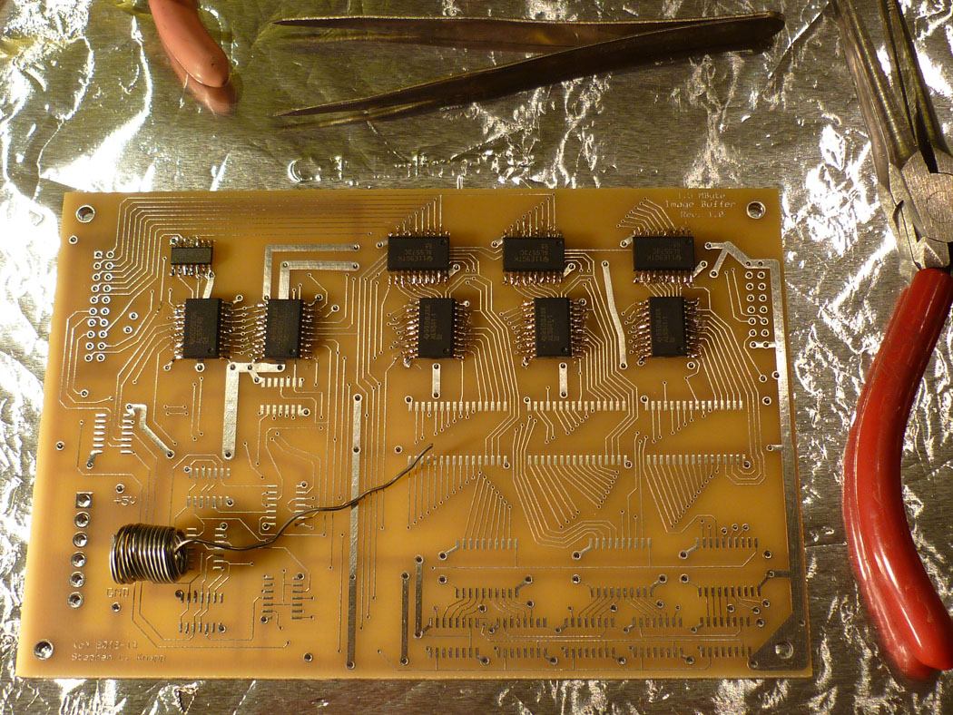
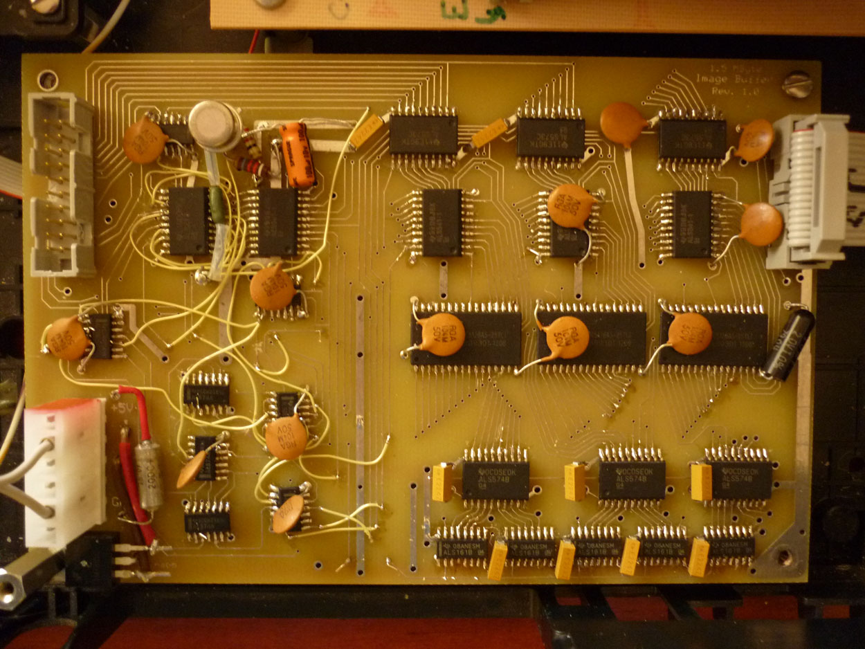
Close up of the Scan Converter board part way through assembly. I am using the smallest Weller soldering iron tip, conical taper to 1/32". The surface mount packages require great care. |
Here is the finished Scan Converter board. I decided to add the 7805 +5VDC regulator at the last minute, seen at the bottom left corner. This required cutting one PCB trace and drilling a couple of holes. Note all the power supply bypass capacitors. |
I had hoped that the PCB would work as is, that it was perfect. This despite dacades of experience with bugs of all sorts in new hardware and software, generally with no single subsystem as complicated as this scan converter PCB. It was totally irrational to be so optimistic, and I knew it down deep. Just who did I think I was? Dick Cheney? Bob Haldeman? Antonin Scalia? Joe Ratzinger? God? - [If any.] - A printed circuit board, especially with tiny devices and many interconnects, is serious work. And any changes require the equivalent of microsurgery using a fine soldering iron and exquisite technique. Even soldering the surface mount ICs to the board is very serious, finicky work.
Here are the mistakes I found: (1) A typographical error in the schematic diagram had interchanged an AND gate and a NAND gate. (2) The rabbit control register (K) was enabled with an inverted signal. (3) Power-on initialization combined with a transistor as a programmable logical OR gate was needed to reset that same control register to zero on start up. (4) Rather embarrasing is the fact that the first ÷3 circuit was incorrect as designed, and I should have used a state table to check it. (5) Most embarrassing of all, one can not gate flip-flop outputs with their own clock signal without getting "cross-over" spikes; imagine, a person of my experience making this blunder, easily fixed with a small delay using spare gates! (6) I found one solder bridge between two IC contacts. The debugged prototype PCB is shown in the image below left. It is easy to revise the PCB layout if I should want more scan converter boards.
|
|
|
Here is the scan converter card after debugging and correcting the design mistakes. The fixes are revealed by the tiny yellow wires that reroute signals. A number of printed traces were cut to disconnect them, and can't be seen in the image. |
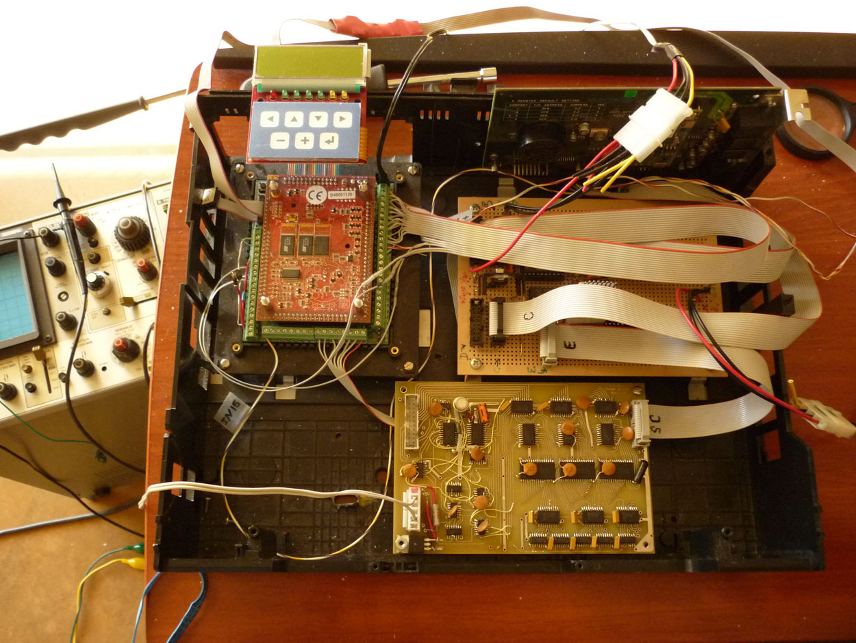
This is a view of the entire Rabbit system as a R&D prototype. The Rabbit single board computer is the reddish card with attached keypad/display on the upper left. The modem card stands on edge at the upper right in dark shadow. The scan converter card is at the lower right. Hidden under the ribbon cables at center is the wirewrapped card that contains the glue logic between the Rabbit and periperals, i.e., the modem and scan converter at the moment. The oscilloscope is visible facing upward below the table. |
Debugging a complex board that contains bi-directional busses with tri-state devices is not easy with only a two channel Oscilloscope, but apparently it is possible. An ambitious circuit, but it works. The basic design is verified. I am happy, if not quite humbled. But I know that everyone is used to this last condition. Now it is on to the Imager Board!
Description of the Imager board goes here.
[I started testing the system using two land lines to my house, and I got erratic data transfers that seemed to depend on outside temperature. ATT came but could not find the problem (they only guarantee voice frequencies.) I got discouraged. So, for now the work is on hold until the rainy season.
|